Sunday, July 25, 2010

How Much Is A Haircut In Bench Fix

Vishay Siliconix Releases Industry's Smallest and thinnest N-Channel Chipscale Power MOSFET mm2 With 0.64-TESTER


MALVERN, PENNSYLVANIA — July 26, 2010 — Vishay Intertechnology, Inc. (NYSE: VSH) today unveiled the industry's smallest and thinnest n-channel chipscale power MOSFET and the first with a sub-1-mm2 outline. The 20-V MICRO FOOT® Si8800EDB combines an ultra-small 0.8-mm by 0.8-mm outline with a height of 0.357 mm to save space in portable electronics.
As portable devices become more compact, the size of components becomes critical, as PCB areas are extremely limited due to the space taken by keypads and batteries. With its ultra-small outline and height, the
Si8800EDB is 36 % smaller and 11 % thinner than the next smallest n-channel device in a chipscale package, allowing for the creation of more compact end products with increased functionality.
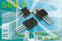
The chipscale packaging of the
Si8800EDB provides an extremely low on-resistance per area due to its packageless technology and increased die area. The MOSFET offers maximum on-resistance values of 80 mΩ at 4.5 V, 90 mΩ at 2.5 V, 105 mΩ at 1.8 V, and 150 mΩ at 1.5 V.
Typical applications for the new device will include load switches and small signal switching in portable devices such as cell phones, PDAs, digital cameras, MP3 players, and smart phones. The
Si8800EDB 's low on-resistance prolongs battery life between charges in these products.
The
Si8800EDB features typical ESD protection of 1500 V, is compliant to RoHS Directive 2002/95/EC, and is halogen-free according to the IEC 61249-2-21 Definition.
Samples of the new power MOSFET are available now. Production quantities will be available in Q2 2010, with lead times of 16 weeks for larger orders.
Vishay Intertechnology, Inc., a Fortune 1,000 Company listed on the NYSE (VSH), is one of the world's largest manufacturers of discrete semiconductors (diodes, MOSFETs, and infrared optoelectronics) and passive electronic components (resistors, inductors, and capacitors). These components are used in virtually all types of electronic devices and equipment, in the industrial, computing, automotive, consumer, telecommunications, military, aerospace, power supplies, and medical markets. Vishay's product innovations, successful acquisition strategy, and "one-stop shop" service Have made it a global industry leader. Vishay Can Be found on the Internet at
http://www.vishay.com .
Subject: ESS.
Student: Pedro Jose Contreras Urbina

Orkester Sound Bank Cd Reason

New 500-V Vishay Siliconix N-Channel Power MOSFETs Feature Low 0555-Ω On-Resistance and Improved Gate Charge of 48 nC in TO-220, TO-220 FULLPAK, and D


MALVERN, PENNSYLVANIA — July 12, 2010 — Vishay Intertechnology, Inc. (NYSE: VSH) today released three new 500-V, 12-A n-channel power MOSFETs with ultra-low 0.555-Ω maximum on-resistance at a 10-V gate drive, and an improved gate charge of 48 nC in TO-220, TO-220 FULLPAK, and D²PAK (TO-263) packages.
The low on-resistance of the
SiHP12N50C-E3 (TO-220), SiHF12N50C-E3 (TO-220 FULLPAK), and SiHB12N50C-E3 (D²PAK) translates into lower conduction losses that save energy in power factor correction (PFC) boost circuits, pulsewidth modulation (PWM) half bridges, and LLC topologies in a wide range of applications, including notebook computer AC adapters, PC and LCD TVs, and open-frame power supplies.
In addition to their low on resistance, the devices feature a gate charge of 48 nC. Gate charge times on-resistance, a key figure of merit (FOM) for MOSFETs used in power conversion applications, is a low 26.64 Ω-nC.
The new n-channel MOSFETs are produced using Vishay Planar Cell technology, which has been tailored to minimize on-state resistance and withstand high energy pulses in the avalanche and commutation mode. Compared to previous-generation MOSFETs, the
SiHP12N50C-E3 , SiHF12N50C-E3 , and SiHB12N50C-E3 offer improved switching speed and losses.
The devices are compliant to RoHS Directive 2002/95/EC and 100 % avalanche- tested for reliable operation.
Samples and production quantities of the new power MOSFETs are available now, with lead times of 8 to 10 weeks for larger orders.
Vishay Intertechnology, Inc., a Fortune 1,000 Company listed on the NYSE (VSH), is one of the world's largest manufacturers of discrete semiconductors (diodes, MOSFETs, and infrared optoelectronics) and passive electronic components (resistors, inductors, and capacitors). These components are used in virtually all types of electronic devices and equipment, in the industrial, computing, automotive, consumer, telecommunications, military, aerospace, power supplies, and medical markets. Vishay's product innovations, successful acquisition strategy, and "one-stop shop" service have made it a global industry leader. Vishay can be found on the Internet at
http://www.vishay.com .
Asignatura: EES.
Alumno: Pedro Jose Contreras Urbina

Spiderman Wrestling Scene

Heat treatment


The mechanical properties of a material depend both on its chemical composition and crystal structure have. Heat treatments change the crystalline structure without altering the chemical composition, giving the material a specific mechanical properties, through a process of successive heating and cooling to achieve the desired crystal structure.
These features are:
Wear resistance: The resistance of a material to be left to erode when in contact friction with another material.
Toughness: The ability of a material to absorb energy without producing cracks (impact).
Machinability: The facility has a material to allow the machining by chip removal.
Hardness: The resistance of a steel to penetrate himself. Is measured in Brinell (HB) or units Rockwell C (HRC) through the test of the same name.

The mechanical properties of alloys of the same metal, and in particular of steel lies in the chemical composition of the alloy that the form and type of heat treatment to which they are subjected. Thermal treatments modify the crystal structure formed by the steel without changing the composition their chemical.
This property of having different grain structures with the same chemical composition is called polymorphism and is what makes the heat treatments. Technically, the polymorphism is the ability of some materials have different crystalline structures, with a unique chemical composition, diamond and graphite are carbon polymorphisms. The α-ferrite, austenite and δ-ferrite are polymorphisms of iron. This property in a pure chemical element called allotropy.
Steel is an alloy of iron and carbon containing other alloying elements, which confer specific mechanical properties for use in the metalworking industry.
The other main elements of composition are chromium, tungsten, manganese, nickel, vanadium, cobalt, molybdenum, copper, sulfur and phosphorus. These are chemicals that are called steel components, and different crystal structures or combination of constituents.
constituent elements according to their percentage, offer specific features for certain applications, tools, knives, stands, etc.. The difference between the various steels, as has been said depends on the chemical composition of the alloy thereof, and the type of heat treatment to which they are subjected.
thermal treatment the material is one of the key steps that can achieve the mechanical properties for which it is created. Such processes involve heating and cooling of a metal in its solid state to change its physical properties. With appropriate heat treatment can reduce internal stresses, grain size, increase toughness or produce a hard surface with a ductile interior. The key of the heat treatment consists of reactions occurring in the material, both in steel and nonferrous alloys, and occur during the heating and cooling of parts, with guidelines and timelines.
To know that the metal temperature should rise for receiving a heat treatment is recommendable to change the phase diagrams as the iron-iron-carbon. In this type of diagrams are the temperatures at which phase changes occur (changes of crystalline structure), depending on the materials diluted.
Heat treatments have become very important in industry in general and with the constant innovations will require metals with high resistance to wear and stress. The main thermal treatments are:
Temple: Its purpose is to increase the hardness and strength of steel. To this end, the steel is heated to a temperature slightly higher than the upper critical Ac (between 900-950 ° C) and then cooled more or less quickly (depending on the characteristics of the piece) in a medium such as water, oil, etc. .
Tempering: This only applies to pre-hardened steels and slightly decreased the effects of temper, still maintains the hardness and increasing toughness. Tempering is able to decrease the hardness and strength of hardened steels, has eliminated the problems created in the temple and improved toughness, leaving the steel with the desired hardness or resistance. Temple differs fundamentally in terms of maximum temperature and cooling rate.
Annealing: It's basically a warm up to austenitizing temperature (800-925 ° C) followed by slow cooling. With this treatment was possible to increase elasticity, while decreasing the hardness. It also facilitates the machining of parts to homogenize the structure, refine grain and soften the material, eliminating the bitterness produced by cold work and internal tensions.
Standard: The purpose leave a material in a normal state, ie, absence of internal stresses and a uniform distribution of carbon. It is usually used as a pretreatment to hardening and tempering.

Maria Linares EES secc1
19881179

Bible Quotes For Christian House Warming

driver driving


lead metals, the theory bands because there is no separation between the valence band and conduction bands, whereas in the insulating these bands are separated and need to have an excess of energy to drive. Natural polymers are insulators, due to the interaction of alternating single and double bonds create a space between the bands "Homo" and "Lumo", ie between the valence band and conduction. Through
doping is achieved the creation of carriers 'free' acting either in oxidation or reduction. Radicals are formed cations or anions.
The task of the doping agent is added or removed electrons in the polymer chain through a redox reaction.
As in traditional semiconductors, we can talk about doping n and p, where P is an oxidative doping and n is a reductive.
With doping fail to make permissible energy levels intermediate between bands, where the radicals, cations or anions allow the flow of electrons.
If the radical is neutral, then called neutral soliton, however are also possible without a radical localized loads, these are called soliton positive (cation) and negative soliton (anion).
electrical conductivity in polymers is related by the following equation: where:
n: Density charge carriers (holes / electrons)
e: Cargo carriers
μ: Mobility of charge carriers
features of freight transportation are affected by the effects of disorder, so a greater driving produces less entropy, however produce a completely ordered polymer is impossible, at least in the short term due to relaxation processes. For example, poly (3-alkyl thiophene) increases the conductivity of 10-5 to 10-2 cm2/Vs when the molecules are arranged.
While conventional metals and semiconductors decrement its conductivity with increasing temperature, the polymer conductivity increase with increasing temperature. This is achieved because the energy required to achieve the delocalization of the charges and is very easy for them interchangeably between segments of the chain.
Examples of polymers that are used as semiconductors:

Maria Linares 19881179
secc1 EES

Dress Up As Albert Ei


Conducting polymers, also called synthetic metals were discovered in 1974 and since then have generated great interest and rapid growth in electronic engineering thermoplastics.
Most produced organic polymers are excellent electrical insulators. Conductive polymers, almost all organic, have delocalized bonds (often in an aromatic group) forming a structure similar to that of silicon. When voltage is applied between the two bands increases the electrical conductivity, are therefore transistors. Almost all known conducting polymers are semiconductors with its banded structure, although some drivers behave as metals. The main difference between conducting polymers and inorganic semiconductors is the mobility of electrons, until recently, much less conductive polymers - a gap that science continues to shrink. Besides its fundamental interest in chemistry, this research has led to many new applications such as light emitting diodes, numerous video screens, the new markings on the products in supermarkets, the processing of photographic film, etc..
Plastics drivers have a great future in information technology.
In the 1970, three U.S. scientists showed that doping polyacetylene film (in this case, oxidizing it with iodine vapor), its electrical conductivity increased a thousand times, comparable to that of metals such as copper and silver. The optical properties of materials were also amended and emitting light.
for the discovery and development of conductive polymers, particularly of polyacetylene doped with iodine was awarded the Nobel Prize in chemistry in 2000 to Alan J.
Heeger. USA, University of California, Santa Barbara. Alan G.
MacDiarmid. U.S. and New Zealand, University of Pennsylvania.
Hideki Shirakawa. Japan, Tsukuba University, Tokyo.
The main advantage of the polymers is their ease of production. Conductive polymers are made of simple plastic and therefore combine the flexibility, strength, elasticity of elastomers with the conductivity of a metal or a doped hybrid polymer.

Maria Linares 19881179 EES
secc1

How Much Can I Sell Pearls For

Polymer Polymer Polymer


semiconducting polymers act similarly to semiconductors doped with silicon or germanium. Its conductivity is in the intermediate range between insulators and conductors. There are 3 types of semiconductors: Expromero, Ipromero and Uimero.
The semiconducting polymer is an effect due to the delocalization of π electrons in an alternating sequence of single and double bonds, for example: In 1975 Hideki
Shirikawa prepared a fully formed by chains attached in the trans position, which conjugated π electrons were therefore with relocation, formed polyacetylene films are already treated them with halogen, halogenation and dehalogenation.
polymer chains to analyze the planned use of infrared spectrum analysis, however, the spectrometer detected no spectrum of the material, but an absorption of 100% when the halogen chlorine was added. Shirikawa acknowledges that at first thought that bleach may be a carrier of cargo and thus be the first conductive polymer history. MacDiarmid and Heeger
found that the polyacetylenes of Shirikawa could be doped with: I2, Br2, AsF5, etc.
The links could be cis or trans, while bonds were conjugated.

Maria Linares 19881179 EES
secc1

Monique Alexander Watch Online

amorphous semiconductor


If the system is amorphous polymer, then no with the anchor points of the crystal structure and the only way to ensure the stability of the temporary is through chain entanglements (physical entanglements and chemical cross-linking does not), plus the ability of the state entrecruzamiento.En vitreous, the movements of long-chain segments are frozen, the movements of these segments depends on an activation temperature that leads to a state rubberized polymer, elastic rotation about the carbon bonds and the movement of the chains are no longer strong enough to accommodate disabilities and to acquire the conformation requires less energy, then chains "unravel" forming random strings without a warrant and therefore more entropy.
If a polymer sample is stretched for a short time in the elastic range, to eliminate the burden, the sample recovered its original form, but if the charge remains for a long enough period, the chains are rearranged and the original form is not recovers the result is an irreversible deformation, also called relaxation process (in this case: English creep or creep).
a polymer to make this the thermal effect of memory, it is necessary to set anchors the strings to avoid these relaxation processes that modify the system.The inelastically amorphous polymers do not have a crystallization temperature (Tm) and the semi-crystalline and have only a glass transition temperature (Tg). This strongly influences the behavior of polymer systems with memory.
is necessary to take into account that a system of self crystalline copolymers alone can be treated with the copolymer loses its crystallinity and crossovers is practically amorphous.
An amorphous polymer crosslinking depends on the level or degree of polymerization, to present this effect. In the case of poly (norbornene) is a linear polymer, amorphous, containing 70 to 80% of trans bonds in commercial products, molecular weight of about 3x10⁶ g mol-1 and Tg approximately 35 to 45 ° C. Because it reaches an unusually high degree of polymerization can be trusted in the entanglements of the chains as anchors to achieve the thermal effect of memory. Therefore this polymer depends solely on physical anchor points. When heated to Tg, the material changes abruptly from a rigid state to a state rubberized (softens). To achieve the effect, the form must be changed quickly to avoid the rearrangement of polymer chain segments and immediately cool the material with high speed also below Tg. By heating the material back to Tg is observed recovery of the original shape.

Maria Linares 19881179 EES
secc1

Hp 1500 Windows 98 Driver

way memory effect induced heat


unidirectional effect heat-induced memory effect is classified into new materials called smart. Polymers with thermal memory effect are new materials, whose applications are being studied recently in different fields of science (eg medicine), communications and entertainment.
reported systems are currently used commercially. However, the possibility of scheduling other polymers are present, due to the amount of copolymers can be designed: the possibilities are almost infinitas.Los polymers with thermal memory effect are those polymers that respond to external stimuli and because of this are capacity to change its shape. The heat-induced memory effect is a combination of proper processing and system programming.
This effect can be observed in polymers with very different chemical composition, which opens a great opportunity to aplicaciones.En the first step polymers are processed by common techniques such as injection or extrusion, thermoforming, at a temperature ( Talta) to which the polymer melts, resulting in a final form called "permanently."
The next step is called system programming and includes heating the sample to a transition temperature (TTrans). At that temperature the polymer is deformed, reaching a form called "temporary." Immediately after the temperature is lowered the sample.
The final step includes the recovery effect of permanently. The sample is heated to the temperature of transition (TTrans) and soon observed the recovery of permanently.
This effect is not a natural property of the polymer, but results from an appropriate programming of the system with the right chemistry.
For a polymer this is necessary for this effect has two components at the molecular level: links (chemical or physical) to determine the permanent and segments "triggers" TTrans for a temporary fix.

Maria linarez 19881179 EES
secc1

Who Can You Give A Counseling Statement To? Army'

super-elastic behavior of shape memory polymers crystallize


The SMA has two types of special behaviors, which in reality are two expressions of the same phenomenon: The shape memory and super elasticity . In both cases, the behavior is the product of a phase transformation without diffusion, martensitic type, in which the order to nearest neighbors is not lost. Strictly speaking, the order itself is lost, not lost are the neighboring atoms. If an atom has been a first group of neighbors, their position in the second state is different, but the neighbors do not change.
One way to see the shape memory effect is in principle the material is in its high temperature phase. By lowering the temperature the transformation to martensite. If such material is now deformed by twinning deformation occurs, ie, again the short-range order is not lost and the first neighbors are the same as shown in Fig. When the material temperature rises again, the material returns to the high temperature phase with the way it was before the deformation. If this same process looking at a graph of stress-strain after cooling, in a first stage, linear behavior is aware of an elastic behavior. Reached a critical stress, deformation continues without increasing voltage or a very smooth voltage rise.
In a third stage, after reaching a critical strain, the strain begins to increase again linearly with a slope similar to that showed in the beginning.
If before reaching the critical strain, the tension relaxes the specimen retains a permanent deformation. Now if the specimen is heated to over a certain temperature characteristic of the alloy (As), begins to recover the deformation that remained until, when the temperature exceeds another critical temperature (Af) which also depends on the alloy and heat treatments, we found that there is no longer the specimen deformation and is in its original dimensions. This behavior is known as "Shape Memory."
In the same alloy but with different mechanical or thermal treatments, with the addition of very small amounts of alloying elements, it may happen that in the tensile test at room temperature, the behavior of the specimen is as shown in Fig. As in the case of shape memory behavior, also seen here as part of achieving a certain tension, the continuous deformation no significant increase in tension. But in this case, to ease the tension, we see a hysteresis loop that ends with almost no permanent deformation. In this seemingly plastic deformation behavior then full recovery is called "super elastic" or "Pseudo plasticity."

Maria Linares 19881179 EES
secc1

Tanya Huff Blood Series Online


polymers that can crystallize are (with the exception of PP) guarantee of obtaining this effect, mainly due to management capacity, which is reflected in crystallinity, the crystals have an affinity for their constituents and form new bonds they manage to anchor forces provide stability to the form temporal.Para analyze the behavior of crystals in this type of polymers used technique WAXS and DSC These techniques help to determine what percentage of the polymer are crystals and how are they organized. This is because the crystallinity decreases as increasing the cross, as the chains lose the ability to accommodate and order is essential to the crystallinity. A second problem
present to crosslink the molecules is the fuse, since an excess of crosslinking adjust the molecule so that leaves to melt (like a heat-stable) and therefore can not obtain a temporary basis.
curing control either electromagnetic waves or peroxide is very important as it increases and decreases TTrans crystallinity, factors in the memory effect.
For semicrystalline biocompatible systems such as poly (ε-caprolactone) and poly (n-butyl acrylate), crosslinked by photopolymerization has been reported that the crystallization behavior is affected by rapid cooling, as in any other semi-crystalline polymer , but the heat of crystallization remains independent of the speed of cooling. The
influence of cross-linking of molecules, rapid cooling and crystallization behavior are unique to each system and impossible to list because the possibilities are almost endless synthesis.
crystallizable polymers such as oligo (ε-caprolactone) segments can be amorphous and poly (n-butyl acrylate) and molecular weight ratio of each determine the behavior of the system in the planning of temporary and recovery permanent form.

Maria Linares 19881179 EES
secc1

Frequency Satellite Astra Hindi Chenal


is known most common materials as steel, that the conversion rate without diffusion martensitic have a degree of progress that depends only on the temperature. That is, exceeded a certain speed of cooling required to grow non-nuclear and equilibrium phases, the high temperature phase (austenite steel) without diffusion transforms into a new phase (martensite BCT). The percentage of transformed material is related to the temperature at which cooling ends. Within the group of alloys with phase changes occur without diffusion, the temperature at which transformation begins as the alloy cools, it is called Ms (martensite start) and the temperature at which no longer show phase changes as long as the cooling process continues, it is called Mf (martensite finish). If cooling is interrupted, that is, if the temperature remains constant during a finite time, transformation does not evolve, but maintains the percentages of phases corresponding to that temperature. Conversely (and not in the case of steel, but in general), when heating the alloy, and a temperature exceeding As (austenite start) the alloy begins to transform to the primary phase, or high temperature and finished to transform when the temperature exceeds Af (austenite finish) or what is, when the temperature is greater than Af all the alloy is in primordial phase high temperature.

Maria Linares 19881179 EES
Sec 1

Basketball Cemented Court Estimate

Transformations without diffusion thermal memory effect (metals)


The thermal effect of memory is a specific effect of the so-called smart materials as artificial muscles and other materials , producing a reaction to a stimulus.
way memory effect was first observed by Chand and Read in 1951 in a gold-cadmium alloy, and in 1963, Buehler et al. described this effect in nitinol, an alloy of nickel-titanium equiatómica.
This effect metals and ceramics is based on a change in the crystalline structure called martensite phase transition. The disadvantage of these materials is that it is a mixture equitaómica and deviations of 1% change in the composition of the transition temperature at about 100 K.
Some metals and ceramics have the effect bidirectionally, which means that at a certain temperature has a form and it can be changed by changing the temperature, but if the first temperature is recovered, also the first form is recovered. This is accomplished by training the material for each shape at each temperature.
metals and ceramics thermally induced two-way effect memory have been widely used in medical implants, sensors, transducers, etc. Many have, however, a risk due to its high toxicity.
The shape memory alloys (SMA) have gained considerable commercial interest in recent years due to the wide range of functions that can perform in the field of medicine, dentistry and electronics applications. Within the group of alloys which has the shape memory phenomenon highlights which are alloys of nickel and titanium. The shape memory effect and super elasticity of the nickel-titanium alloy was discovered by Buehler et al in 1963 The most famous of these alloys was designed and released by the laboratories of the U.S. Navy in the 70's and is named in reference to the laboratories of that institution: Nitinol (Nickel Titanium Naval Ordnance Laboratories). Worldwide, there are many companies engaged in the production of the alloy. However, companies that manufacture products with high added value engineering are very few. As an example we can cite the Nitinol tube production is reduced to five companies worldwide. [2] The complexity for the working and complications at the time of production make products require many hours of engineering design process, and often times longer tuning. While the SMA are studied by science in its capacity as basic and applied science, relevant publications tend to show a little too basic physical, or sometimes, when referring to industrial data, are petty and inaccurate. The first pieces of Nitinol were manufactured in 1991 by Raychep corp. a set of steerable periscopic devices. Today in the market are stents1 with superelastic behaviors that replace the functions of the existing stents. Some other applications that are made of Nitinol can be catheters, orthodontic components in general, and other devices that can be named. Maria Linares
19881179 EES secc1

Midnighthot Tv In India

Area MOS-FET TRANSISTOR Special

this circuit in the figure below, consists of an oscillator stage followed by an amplifier stage, is simple and has a status indicator uses few components and easy to find.

So we use the oscillator to generate the frequency that allows us to determine whether the transistor under test is capable of amplifying the signal, if so transistor in good condition, otherwise, buy another.
Operation:
As foreshadowed, the circuit tester is an astable oscillator formed by the two gates ICA-ICB investors in the scheme and the frequency of oscillation is determined by the values \u200b\u200bof R1 and C1, in this case a frequency near 120 Hz to avoid possible the annoying flash.
If you want to change the frequency, can be done by setting potentiometer R1, arranged for this purpose. The frequency can be calculated by: f = 1 / (0.7 x R1 x C1), where R1 is in Ohms and C1 in farads.
C1 should be less than 10uF to avoid as much as possible the "high leakage currents" to be presented, comparable to the initial charging current of the capacitor in many cases. The capacitor acts like a short circuit. Because the investor has 6 CI4049B have been used in parallel pairs as you can see, so you get more intensity and chargeability, ensuring the necessary current to drive the LED's. Oscillation obtained
attacks the input of a pair of separators investors to not load the oscillator and heads the terminals of the transistor FET, but with a lag of 90 °, in another couple of investors, ensuring a flow of current DS (drain-sink) in each half of the oscillation and SD in the half cycle following when they stay active pusher This will excite the corresponding LED indicating its polarity (Canal N or P channel) and if in good condition.

Subject: ESS.
Student: Pedro Jose Contreras Urbina
Source:
http://www.fortunecity.es/felices/barcelona/146/3ds/tutores/mosfet_test.html

Saturday, July 24, 2010

Babysoft. Myarbourne.com

: How to make a wind turbine (windmill or wind turbine). WITH ANALOG MULTIPLIER


Following the line of inventions of renewable energy, today I bring you another special, this time to make a wind turbine. Like the previous special make a solar panel , this is also the same author, and we have commissioned to translate.
The main characteristics of this wind turbine can vary by type of motor or generator that you installed, but normally will be about efficient voltage 12V. Enjoy this invention making it as much as I translated for you:
After many searches for information all over the Internet, I realized that all designs had five things in common:
A generator.
Palas.
guidance system into the wind (Timon).
A tower to raise the turbine to where the wind.
batteries and electrical control system.
Organizing a little issue, I managed to reduce the project to just five systems, attacking slowly and one by one, not at all complicated. I decided to start the generator. Looking at the projects of other people online, I realized there were people who decided to become its own generator, wearing other resident energy permanent magnet motors, and others simply looking for a generator. So I decided to look for. Many people used
engines tape drives of old computers. The best for this are the 99-volt Ametek continuous work well as generators. Unfortunately, they are very hard to find, although you can always try other similar models of Ametek (In
eBay , for example). Here is a site (in English) that discusses the strengths and weaknesses of the Ametek generators, very complete truth.
There are many other makes and models permanent magnet motor than the Ametek, but may not work as well, note that the permanent magnet motors were not designed to be generators. Normal engines when used as generators, must be driven much faster than its rated speed of operation to achieve a production similar to that of normal operation. With these data, we can draw a conclusion, we are looking for is an engine of stress with low speed. Away from engines with many revolutions and little tension, because it will be useless. What we seek, more or less, is an engine that gives us a useful voltage 12 V with a speed very low (325 rpm). When you have, for the test, connect to a 12 v bulb give a sharp turn to the engine by hand, if we really work, the bulb should go on as usual.
Subject: ESS.
Student: Pedro Jose Contreras Urbina

How Do You Get The Cut In Pokemon Pearl

MOSFETS.


Summary: ANALOG MULTIPLIER WITH MOSFETS. MEDIA PRESENTS LINEAR VARIABLE RESISTIVITY MOSFET varies linearly TO STRENGTH "I" OUTPUT AS A FUNCTION OF A SYMMETRIC INPUT VOLTAGE SOURCES "V2" Y "-V2" VOLTAGE AND INPUT VOLTAGE FROM A SINGLE SOURCE " V1 input voltage operatively associated with SYMMETRIC INPUT VOLTAGE FROM SOURCES "V2" Y "-V2" TENSION BEARING MEDIA MOSFET LINEAR VARIABLE RESISTIVITY a node "A" FOR YOUR CAUSE THROUGH STRENGTH "I" OUTPUT WIDE. OPERATIONAL AMPLIFIER UNIT ALSO INCLUDES AN ELEMENT "Z" FEEDBACK CONNECTED BETWEEN THE INPUT TERMINAL INVESTMENT AND OUTPUT TERMINAL OPERATIONAL AMPLIFIER "U", PRODUCING THE TERMINAL AN OUTPUT VOLTAGE "VO." Applications, including, HYBRIDS FOR AN ANALOG-DIGITAL NEURAL SYNAPSE ARTIFICIAL.Solicitante: KOREA TELECOMMUNICATION AUTHORITYNacionalidad: KRInventor / s: IL SONG, HANFecha Application: Publication 16/07/1992Fecha Concession: 01/09/1996Fecha of Concession: 19/07/1996Clasificación Principal: G06G7/02 , G06G7/163

Subject: ESS.
Student: Pedro Jose Contreras Urbina
Source: http://patentados.com/invento/multiplicador-analogico-con-mosfets.html

Make Hair Look Messy Product

What is better a valve or transistor amp ...

I prefer valves, although might not want to complicate your life yte decide by a transistor amp with the latest technology modulacion.Te explain that ....


VALVES: (Tubes, Vacuum Tube, Triode, Pentode, etc.) Tubes operate by thermionic emission of electronesdesde a filament or cathode, controlled by a rejillay collection on a plate. Some tubes have morethan grid amplificadoresseparados Some have two elements in a glass envelope. These dual function valvulassuelen peor.Las characteristics of tubes varies widely dependiendodel selected model. In general, tubes are large, fragile, pretty, run hot and need variossegundos before operating. Tubes have gananciarelativamente low, high input impedance, low input capacity up, and the ability to withstand abuse momentaneos.Las Tubes overload (clip) gently and recuperandos suavemente.Los overload quickly and circuits that do not use tubes are called transistors (or state solid), they do not use devices that contienengas (or liquid). The characteristics of tubes tend to change with use (age). Are more susceptible to vibration (called "microphonics") than solid state devices. Lasvalvulas suffer from noise even when used with current filaments alterna.Las valves are designed for operation at higher voltages quecualquier other device, but high corrienteson valves rare and expensive. This means that most valves losamplificadores to use an output transformer. Despite not being specifically a tube characteristic, output lostransformadores added distortion of the second armonicoy show a gradual fall in response to high frecuenciasque is difficult duplicate with circuits.


TRANSISTORS: (BJT, Bipolar, PNP, NPN, Darlington, etc.) Transistors operate by minority carriers inyectadosdesde the emitter to the base that are swept labase through to the collector, controlling the flow of base.Los Transistors are available as PNP and NPN devices, allowing one to pull the output signal. The transistoresestan also available packaged as matched pairs, emitter follower pairs, arrays of transistors multiplese even as complex "integrated circuits", where estancombinados resistors and capacitors for circuit conseguirfunciones complejos.Como valves, there are many kinds of BTJs disponibles.Algunos have high current gain, while whichothers have lower gain. Some are fast, while others lentos.Algunos handle high current while others tienencapacidades lower input. Some are less ruidoque others. In general, the transistors are stable, last casiindefinidamente, have high gain, require some input Unheard, have low input resistance, higher input tienencapacidad, saturate quickly, and sonlentos to recover from overdrive (saturation). Lostransistores have a wide margin before saturacion.Los transistors are subject to a mode of llamadosegunda failure breakdown, which occurs when the device estatrabajando to high voltage and high current. The segundaavalancha can be avoided by conservative design, WHEREOF gave the first amplifiers transistoresuna bad reputation for reliability. Transistors are tambiensusceptibles of thermal runaway when seus incorrectly. However, the designs prudentesevitan second breakdown and runaway termico.MOSFET (VMOS, TMOS, DMOS, NMOS, PMOS, IGFET, etc.) The field-effect transistors metal-oxide semiconductor usanuna insulated gate to modulate the flow of portadoraprincipal power source to the drain with the electric field creadopor the door. Like bipolar transistors, MOSFETs are disponiblesen P and N. Also like transistors, MOSFETs are disponiblesen pairs and integrated circuits. MOSFET matched seacoplan not as well as bipolar transistor pairs, Peros valvulas.Los match better than MOSFETs are also available in many types. HOWEVER, all have low input current and input bajacapacidad enough. MOSFETs have lower gain, is saturanmoderadamente and recover quickly from saturation. Despite that power MOSFETs have no DC gate current, finite input capacitance means that MOSFETs have a gate depotencia AC finite. The MOSFETson stable and robust. Are not subject to runaway termiconi second breakdown. However, MOSFETs puedensoportar abuse as well as valvulas.JFET: Effect Transistors Junction Field exactamenteigual operate the MOSFET, but do not have a door aislada.Los JFETs share most of the characteristics of losMOSFETs, including available pairs, P and N, ycircuitos integrados.Los JFETs are not commonly available as power dispositivosde. They make excellent preamps Bajoru. The union of the door gives JFETs ingress policer greater capacity than MOSFETs and also prevents them from being used as accumulation or enrichment. JFETs unicamentese deplexing used as circuits or empobrecimiento.Los JFETs are also available as parejasy match almost as well as transistors bipolares.IGBT: (or IGT) Transistors insulated gate bipolar are a combination of unMOSFET and a bipolar transistor. Part dispositivosirve MOSFET as an input device and the bipolar as salida.Los IGBTs are currently available only as a device such as N, P coppers devices are possible in theory. IGBTs are lentosque other devices but offer a low cost, high capacity up current bipolar transistors with low Unheard input and low input capacitance of the saturation MOSFETs.Sufren much or more than lostransistores bipolar, and even suffering from second avalanchaRaramente used in High-end audio, but sometimes used paraamplificadores of extremely high power. Now the real question: You think that if they are so diversosdispositivos different from each other, one must be elmejor. In practice, each has its weak points fuertesy. Also, because each type of device estadisponible in so many ways, most lostipos can be used in most of the sites exito.Las Tubes are prohibitively expensive for very high power amplificadoresde. Most avalvulas amps deliver less than 50 watts per canal.Los JFETs are sometimes an ideal input device porquetienen low noise, low input capacitance and good acoplamiento.Sin But bipolar transistors have even mejoremparejamiento and profits, so that bajaimpedancia sources, bipolar devices are even mejores.Aun the tubes and MOSFETs have even lower capacity up entry, so for very high output resistance, podrianser mejores.Los Bipolar transistors have the lowest resistance desalted, so they make great output devices. However, the second breakdown and high stored charge weigh in contracuando be compared with the MOSFET. A good design BJT ceunta necesitatener in the weaknesses of BJTs while MOSFET design needs unbu disadvantages MOSFETsLos models require bipolar output transistors Protectionof second breakdown and thermal runaway and this proteccionrequiere additional circuitry and design effort. Insome amplifiers, the sound quality is damaged withthe proteccion.Como already said, there are more differences between individual designs, whether valves and transistors, which is between tube and transistor designs generalesentre. You can do a good amplificadorde either, and you make a lousy amp though tambien.A tubes and transistors clip differently, clipping will be rare or absent in a good amp, so this difference should be taken into people cuenta.Alguna claim that tubes require less or no unarealimentacion while transistoresrequieren significant feedback. In practice, Disable ALL amps require some feedback, seatotal, local, or just "degeneration." The feedback essential in amps because it makes amplificadorestable with temperature variations and manufacturable in spite of changes in componentes.La Feedback has a bad reputation because Queuña badly designed feedback system can vary dramatically passed. Some older designs usabanexcesiva feedback to compensate for not linealidadesde lousy circuits. Realimentacionesbien amplifiers that are stable and have designed a very small sobreimpulso.Cuando amps were first transistor, were worse than the best tube amps of aquellosdias. The designers made many mistakes with nuevastecnologias as they learned. Today, designers sonmucho more sophisticated and experienced in those days 1960.Debido to low internal capacitances, amplificadoresa valves have characteristics very lineales.Esto input makes tube amps tolerant alimentary easy to sources of high output impedance, talescomo other tube circuits and volume controls Dealt-impedance. The Transistor amps may have an essential high coupling between the input and output and may have an essential lower input impedance. However, some circuits tecnicasde reduce these effects. Even some transistors amplificadoresde completely avoid these problems by using circuits entrada.Hay buenosJFET as many exaggerations, errors as well as many leyendassobre the subject. Indeed, a good FET designer can make unbu FET amplifier. A good tube designer puedehacer a good tube amp, and a detransistores good designer can make a transistor amp HiThere. Many designers mix components to use them as they are mejores.Al As with all engineering disciplines, losbuenos amp design requires a broad conocimientode the characteristics of components, failure dediseño amplifiers, sourceofgrowthwas characteristics of the signal, characteristics of the loads, and signal caracteristicasde misma.Otro issue, we lack a good set of medidaspara rate the quality of an amplifier. The frequency response, distortion and signal-noise ratio give hints, but by themselves are insufficient to qualify people swear elsonido.Mucha tubes sound more "tube" and lostransistores sound more "transistor." Some people add a valve uncircuito their transistor circuits to darlesalgo sound "tube" Some people say they have measured a distinct diferenciasentre the distortion characteristics of amplificadoresde valves and transistors. This could be causadopor the output transformer, the function of transferenciade the tubes, or the choice of the topology of amplificador.Los tube amps rarely have enfrecuencia response as flat as the flattest detransistores amplifiers, due to the output transformer. However, the frequency response of good tube amps extremely good.
Subject: ESS.
Student: Pedro Jose Contreras Urbina

Brazillian Hair Removal Funny Sayings

ZERO FEEDBACK

In the mid seventies was a concept developed in Europe about the advantages of low global feedback amplifiers. It is said that feedback amplifiers have problems because the signal fed back "takes" a while back at the entrance and this causes loss of quality and ¨ ° to sound natural. You said that amortiguaiento factor (damping factor) improved low-feedback amplifiers.
Today the discussion continues, but restricted to the amount of feedback.
The reality is that you can get excellent results with a synergy of local and global feedback feedback. To extend the latter
explore a bit the concept of delay between input and output. " Electromagnetic energy travels in a conductor at a speed of 230,000 km / s. This means say that a cable of 23 cm long (distance comparable to the size of an amplifier) \u200b\u200bis traversed by an electromagnetic wave in 1 nanosecond, which is the period of a 1Ghz signal. A 20,000 Hz signal has a wavelength within a conductor of 11.5 km or 11,500 meters. Therefore the concept of "delay" is not applicable to an audio amplifier, but try running a 11,500 m long cable into your amplifier.
When feedback or an article you read damping factor "delay" so read is "phase", and the phase is inherent in the reactors' own input devices drivers and output and transfer characteristics of the fed back locally and globally.
seriously can not be assessed if the feedback is high or low if you consider what kind of devices and topologies are involved in the design. Let

History:
problems with the amplifiers of the early 70's are two: the design criteria and semiconductor devices that were available.
be considered an audio amplifier and an operational amplifier that is high gain and a dominant pole, generally in the input stage, which by the amp stable to close the loop in any condition. Moreover, we see in many designs of an operational period, type UA741, the input of the circuit to take advantage of the differential pair and the dominant pole.
know that a dominant pole at low frequency, usually 10Hz, brings two problems: one consisting of two events of similar nature, the slew-rate and the reduction of intermodulation, and the other, the damping factor degradation by falling the loop gain at medium frequencies.
should be taken into account for the correct understanding that these dynamic processes, such as slew-rate and cutting intermodulation are independent phenomena for feedback, the show, the feedback is cut (see *)
To solve these problems changed the design criteria. Today is seeking the power band width, ie maximum excursion of tension, is greater than the small-signal, ie when it falls midrange 3db. To achieve this criterion
need two things: first input differential pair with discrete components, resistors degenerate emitter, or appropriate local realimenación bias current (see *) and second drivers and output devices very fast ie MOSFETs, to take the pole of the input stage, which is no longer dominant, up to about 15000 Hz
With these two design criteria, the feedback amplifier multiple discrete components and transistors to the output MOSFETs is the best option as the audio amplifier to date.
* A complete analysis can be seen in Gray & Meyer "Analysis and Design of Analog Integrated Circuits" John Wiley and Sons. P. 1977. 541 and following


Subject: ESS.
Student: Pedro Jose Contreras Urbina
Source:
http://www.vn-amps.com.ar/zero.htm

Welcome Message For Beauty Saloon

25W audio amplifier with mosfet output MOSFET

can connect directly to CD players, tuners and tape recorders.
to operate effectively add a 5K potentiometer one end connected to the audio input in the middle leg of the potentiometer connected to C1 and the other end to land that is almost mandatory for this circuitoQ6 and must Q7 and Q9 pequeñosQ8 sinks should be mounted on heatsinks. (appropriate) Adjust R11 so there is no noise, adjust, adjust the current of 100 mA, check the consumption series the drain of Q8 with no input signal. the trimer (R11) is attached to the center leg connected to one of the trimer extrmos so you can vary the current.
components: Q1-Q5______BC558B
45V 100mA Low noise High gain PNP transistors

Q6_________BD140 80V 1.5A PNP Transistor

80V 1.5A NPN Transistor Q7_________BD139

Q8_________IRF530 100V 12A N-Channel Hexfet Transistor

Q9_________IRF9530 100V 10A P-Channel Hexfet Transistor

R1,R4_________47K 1/4W Resist.

R2____________4K7 1/4W Resist.

R3____________1K5 1/4W Resist.

R5__________390R 1/4W Resist.

R6__________470R 1/4W Resist.

R7___________33K 1/4W Resist.

R8__________150K 1/4W Resist.

R9___________15K 1/4W Resist.

R10__________27R 1/4W Resist.

R11_________500R 1/2W Trimmer Cermet

R12,R13,R16__10R 1/4W Resist.sR14,R15_____220R 1/4W

R17___________8R2 2W Resist.

R18____________R22 4W Resist. (wirewound)

C1___________470nF 63V Polyester Condensador

C2___________330pF 63V Polystyrene Capacitor

C3, 63V Electrolytic Capacitors C5________470μF

C4, C6, C8, 63V Polyester Capacitors C11_100nF

25V Electrolytic Capacitor C7___________100μF

C9____________10pF 63V Polystyrene Capacitor

C10____________1μF 63V Polyester Capacitor
Thanks I await your prompt response.
Note: the 5 K potentiometer is required on the circuit thanks. haaaa and tablet if possible should be amcho 6cm and 8cm long so many thanks that I restart the other a capacitor and resistor were not connected to anything because now I add the potentiometer to be input
Subject: ESS.
Student: Pedro Jose Contreras Urbina
Source:
http://www.circuitosimpresos.org/2010/07/01/amplificador-de-audio-de-25w/

Barefoot Contessa Peanut Butter Brownies

Vs PWM motor control with MOSFETs

From arg , Mario Sacco brings us this interesting article on control of DC motors by setting "H-Bridge." Well known and
famous "H bridge" or "H bridge" is always the solution in systems where the rotation is an operational necessity. However, the real, physical world presents countless difficulties in operating the H-bridge Starting with the inertia of the mechanical system, through the speed response and ending in the braking process and appropriate detention, we find most of the problems that have been leaving many enthusiasts who are new to the world of robotics and mechatronics. Let us together a bit of theory and practice of this device to move the motors in our future productions.


With this circuit you can control DC motors by injecting a signal PWM can generate with a microcontroller.
The project underlying the control load by H bridge built around MOSFETs. Its implementation is simple and author provides full material: schematic, parts list, PCB files.

Subject: ESS.
Student: Pedro Jose Contreras Urbina
Source: http://www.automatismos-mdq.com.ar/blog/2010/03/control-pwm-de-motores-con-mosfets.html

Looking For Gays In Kolkata

Sub MOSFET AMPLIFIER S-MOSFET Power Bridge Rectifier

Introduction

One day some PCBs and insol an undetermined cause of a PCB of a S-SUB charge went wrong. Lacquer was corrupt the whole side, just the output stage, and right hand only. Like the rest had gone quite well thought of attaching a simple output stage, as he needed an amplifier to make subjective evaluations of sound, along with the monitor.
The result was the S-MOSFET SUB version not can be nothing simpler than an output stage push-pull common-drain MOSFET.
The circuit used is almost the same as in the S-SUB, but with some modification resulting from the output stage employed. Also modified some elements of gain and frequency compensation.
On the right you can see the new circuit.


Topology
Although a priori it easy, an output stage with two transistors, "fat" and a few resistors, in practice it is not so, in fact I had to make a separate PCB because it also incorporates a limitation current.
The first is that the output impedance of the voltage gain stage is very high, and the input capacitance of the mosfet as well. It is not really that of the power BJT (1500-3000pF), but if there is a different feature: as you do not need a driver transistor, the EGV deal directly with that capability. We need this capability in conjunction with high output impedance of the EGV form a pole (lowpass filter behavior) that creates a lag of 90 degrees. If we add the gap resulting from the frequency compensation, we have another 90 º to 180 º invert the output phase. At that time negative feedback ceases to be "negative" and passes to be positive, so that the amplifier becomes unstable and tends to the power rails, and in proper condition ranges (the most normal).
This avoids degenerating the pole, adding a resistor in series with the gates of the output MOS transistors. At audio frequencies this technique has no deleterious effect on the dynamics.
Moreover, the temperature coefficient of the MOSFET is initially negative, charge carriers that use does not generate heat (one of the reasons they do not suffer from secondary breakdown). As I have understood today, there are differences between the temperature coefficient of voltage of strangulation and transconductance. The transconductance decreases with temperature, so that reason can place them in parallel and ideally dispense step allows thermal compensation.

In recent times, practically the only application that uses MOSFET transistors in linear region is the audio and radio, which still survive without rival many vacuum tubes. In all other linear applications with this operation has been replaced by the PWM, more efficient, linear and much higher for low frequencies below 1 kHz and applications requiring high accuracy (0.1% min) and motor control , servos ...
The need to optimize them for switching and a low channel resistance has brought new forms of manufacture: V-MOS-FET Trench, T-MOS-FET ... HEX, and the result is that the voltage bottleneck decreases with increasing temperature, unlike the classic FETs Hitachi, which did not require any thermal compensation. The required temperature compensation is finally adjusted by a VBE multiplier, but degenerated to a diode that is not in contact with the radiator.
HEXFETs The models are of International Rectifier, the famous IRFxxxx. At first, I I used version of IRF640 and IRF9640, two models of 150W TO-220, that will output to 25W more than enough, but there are more suitable as IRFP9240 IRFP240 and also 150W, but in capsule TO-3P.
The difference between these two models is that the TO-3P support more power continuously because the body heat resistant silicon and the radiator is substantially lower. Goes from 1.5 to 1.07, 30% lower. This implies that when the radiator of 0.5 º C / W at 50 ° C in the TO-3P, the silicon transistor will be at 103 º C, while the TO-220 will be 125 º C. The limit is 150 º C, and the colder the transistor will be more linear.

Therefore, it is possible to operate with IRF540 and IRF9540, IRF640 and IRF9640, but I can only recommend and IRFP9240 IRFP240 with powers equal to or more than 80W.Por Finally, the assembly is much simpler because the transistors are mounted on the plate and are attached to the radiator, instead of mounting on the radiator and use cables to connect them to the plate
Subject: ESS.
Student: Pedro Jose Contreras Urbina
Source:
http://www.pcpaudio.com/pcpfiles/proyectos_amplificadores/ssub-mosfet/Ssub_mosfet.html